


Video
Hỗ trợ khách hàng
Danh mục sản phẩm
Hỗ trợ kỹ thuật
Hotline hỗ trợ
0901578086
0901578086
Thống kê truy cập
- Online:
- Số lượt truy cập: 262510
Chi tiết sản phẩm

- DRV8833 Dual Motor Driver Carrier
- Xuất xứ: Pololu - Mỹ
- Giá: Liên hệ
- Tình trạng: Còn hàng
- Lượt xem: 2880
Overview
 |
|
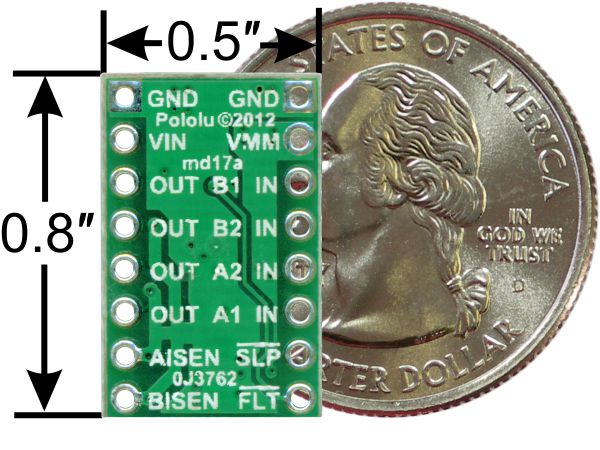
DRV8833 dual motor driver carrier, bottom view with dimensions. |
|---|
Texas Instruments’ DRV8833 is a dual H-bridge motor driver IC that can be used for bidirectional control of two brushed DC motors at 2.7 V to 10.8 V. It can supply up to about 1.2 A per channel continuously and can tolerate peak currents up to 2 A per channel for a few seconds, making it an ideal driver for small motors that run on relatively low voltages. Since this board is a carrier for the DRV8833, we recommend careful reading of the DRV8833 datasheet (1MB pdf). The board ships populated with SMD components, including the DRV8833, and adds a FET for reverse battery protection.
This board is very similar to our DRV8835 dual motor driver carrier in operating voltage range and continuous current rating, but the DRV8835 has a lower minimum operating voltage, offers an extra control interface mode, and is 0.1″ smaller in each dimension; we also carry a DRV8835 dual motor driver shield that is easy to use with an Arduino. The DRV8833 has a higher peak current rating (2 A per channel vs 1.5 A), optional built-in current-limiting, and no need for externally supplied logic voltage.
For a smaller, lower-cost, single-channel alternative to this driver, please consider our DRV8838 carrier, which offers a similar operating voltage range and current capabilities.
For higher-voltage alternatives to this driver, consider our A4990 and DRV8801 motor driver carriers.
Features
- Dual-H-bridge motor driver: can drive two DC motors or one bipolar stepper motor
- Operating voltage: 2.7 V to 10.8 V
- Output current: 1.2 A continuous (2 A peak) per motor
- Motor outputs can be paralleled to deliver 2.4 A continuous (4 A peak) to a single motor
- Inputs are 3V- and 5V-compatible
- Under-voltage lockout and protection against over-current and over-temperature
- Reverse-voltage protection circuit
- Current limiting can be enabled by adding sense resistors (not included)
Using the motor driver
 |
|
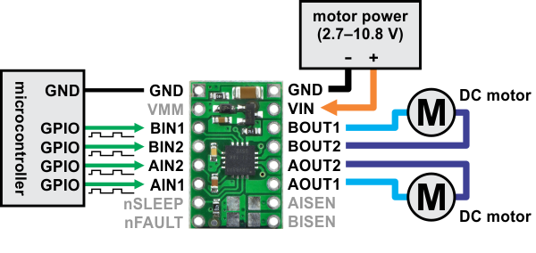
Minimal wiring diagram for connecting a microcontroller to a DRV8833 dual motor driver carrier. |
|---|
In a typical application, power connections are made on one side of the board and control connections are made on the other. The nSLEEP pin is pulled high on the board and can be left disconnected if you do not want to use the low-power sleep mode of the DRV8833. Each of the two motor channels has a pair of control inputs, xIN1 and xIN2, that set the state of the corresponding outputs, xOUT1 and xOUT2; pulse width modulated (PWM) signal can be applied to each of these inputs. The control inputs are pulled low internally, effectively disabling the motor driver outputs by default. See the truth tables in the DRV8833 datasheet for more information on how the inputs affect the driver outputs.
The nFAULT pin is an open-drain output that is driven low by the chip whenever an over-current, over-temperature-or under-voltage condition occurs. Otherwise, it remains in a floating state, so you will need to connect an external pull-up resistor (or use a microcontroller input with its built-in pull-up enabled) if you want to monitor fault conditions on the driver.
Pinout
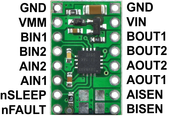 |
| PIN | Default State | Description |
|---|---|---|
| VIN | Reverse-protected 2.7 V to 10.8 V motor power supply connection. Operation with VIN below 5 V slightly reduces the maximum current output. | |
| VMM | This pin gives access to the motor power supply after the reverse-voltage protection MOSFET (see the board schematic below). It can be used to supply reverse-protected power to other components in the system. It is generally intended as an output, but it can also be used to supply board power. | |
| GND | Ground connection points for the motor power supply and control ground reference. The control source and the motor driver must share a common ground. | |
| AOUT1 | The motor A half-bridge 1 output. | |
| AOUT2 | The motor A half-bridge 2 output. | |
| BOUT1 | The motor B half-bridge 1 output. | |
| BOUT2 | The motor B half-bridge 2 output. | |
| AIN1 | LOW | A logic input control for motor channel A. PWM can be applied to this pin. |
| AIN2 | LOW | A logic input control for motor channel A. PWM can be applied to this pin. |
| BIN1 | LOW | A logic input control for motor channel B. PWM can be applied to this pin. |
| BIN2 | LOW | A logic input control for motor channel B. PWM can be applied to this pin. |
| nSLEEP | HIGH | Sleep input: when this pin is driven low, the chip enters a low-power sleep mode. (Labeled SLP on the board silkscreen.) |
| nFAULT | FLOAT | Fault output: driven low in the event of an over-current, over-temperature, or under-voltage condition; floating otherwise. (Labeled FLT on the board silkscreen.) |
| AISEN | Current sense pin for motor A. This pin is connected to ground and does not function by default, but current limiting can be enabled by making the modifications described below. | |
| BISEN | Current sense pin for motor B. This pin is connected to ground and does not function by default, but current limiting can be enabled by making the modifications described below. |
Sản phẩm cùng loại


Đối tác toàn cầu


